What is a Tunnel Diode?
A Tunnel Diode is a heavily doped p-n junction diode. The tunnel diode shows negative resistance. When voltage value increases, current flow decreases. Tunnel diode works based on Tunnel Effect.

The following image shows the symbol of a Tunnel Diode.

Leo Esaki invented Tunnel diode in August 1957. Therefore, it is also called as Esaki diode. The materials used for this diode are Germanium, Gallium arsenide and other silicon materials. Tunnel diode shows a negative resistance in their operating range. So, it can be used as amplifier, oscillators and in any switching circuits.
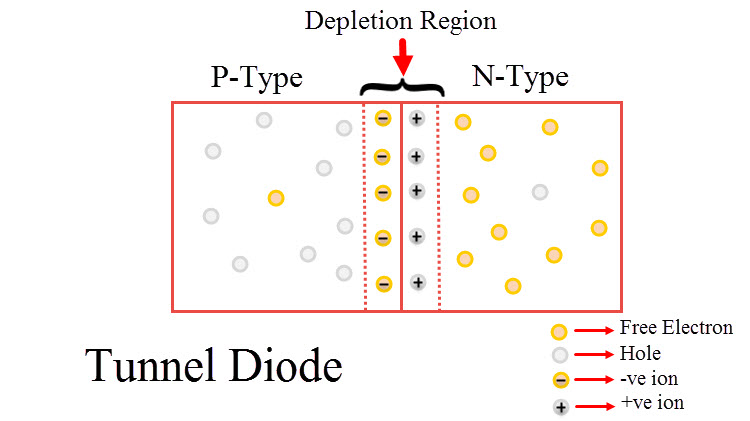
Width of the Depletion Region in Tunnel Diode
When mobile charge carriers both free electrons and holes are missing, the region in a p-n junction has a region called Depletion region. To stop the flow of electrons from the n-type semiconductor and holes from the p-type semiconductor, depletion region acts as a barrier.
Depending on the number of impurities added, width of depletion region varies. To increase electrical conductivity of the p-type and n-type semiconductor impurities are added. A wide and big depletion region is formed when a smaller number of impurities is added to p-n junction diode. At the same time, when a greater number of impurities is added, narrow depletion region occurs.
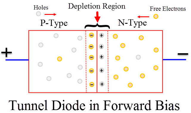
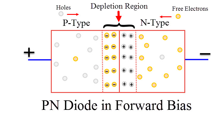
The p-type and n-type semiconductor is heavily doped in a tunnel diode due to a greater number of impurities. Heavy doping results in a narrow depletion region. When compared to a normal p-n junction diode, tunnel diode has a narrow depletion width. Therefore, when small amount of voltage is applied, it produces enough electric current in the tunnel diode.
Tunneling Effect
In electronics, Tunneling is known as a direct flow of electrons across the small depletion region from n-side conduction band into the p-side valence band. In a p-n junction diode, both positive and negative ions form the depletion region. Due to these ions, in-built electric potential or electric field is present in the depletion region. This electric field gives an electric force to the opposite direction of externally applied voltage.
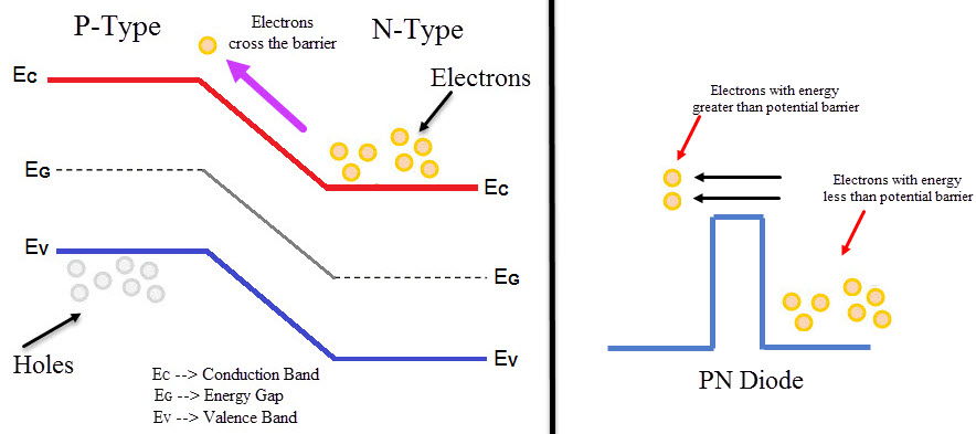
As the width of the depletion layer reduces, charge carriers can easily cross the junction. Charge carriers do not need any form of kinetic energy to move across the junction. Instead, carriers punch through junction. This effect is called Tunneling and hence the diode is called Tunnel Diode.
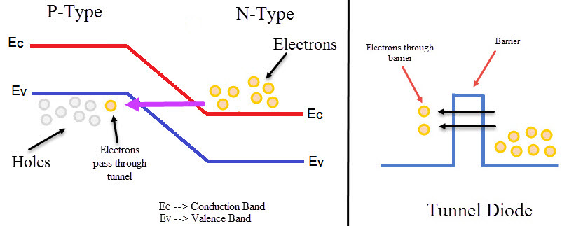
Due to Tunneling, when the value of forward voltage is low value of forward current generated will be high. It can operate in forward biased as well as in reverse biased. Due to high doping, it can operate in reverse biased. Due to the reduction in barrier potential, the value of reverse breakdown voltage also reduces. It reaches a value of zero. Due to this small reverse voltage leads to diode breakdown. Hence, this creates negative resistance region.
Tunnel Diode Working Phenomenon
Unbiased Tunnel Diode
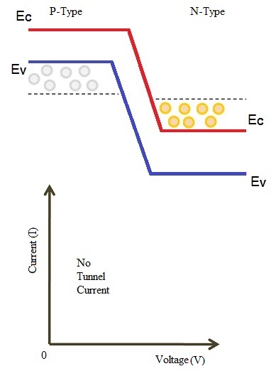
In an unbiased tunnel diode, no voltage will be applied to the tunnel diode. Here, due to heavy doping conduction band of n – type semiconductor overlaps with valence band of p – type material. Electrons from n side and holes from p side overlap with each other and they will be at same energy level.
Some electrons tunnel from the conduction band of n-region to the valence band of p-region when temperature increases. Similarly, holes will move from valence band of p-region to the conduction band of n-region. Finally, the net current will be zero since equal numbers of electrons are holes flow in opposite direction.
P α e (-A *E *b *W)
P – Probability that the particle crosses the barrier
W – Width of the barrier
E – Energy of the barrier
Small Voltage Applied to the Tunnel Diode
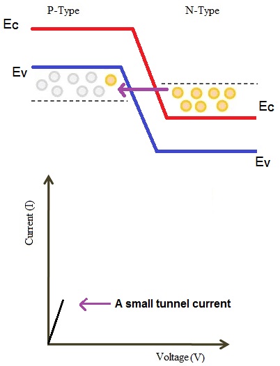
When a small voltage, that has lesser value than the built-in voltage of the depletion layer, is applied to the tunnel diode, there is no flow of forward current through the junction. Nevertheless, a minimal number of electrons from the conduction band of n region will start tunneling to valence band in p region.
Therefore, this movement creates a small forward biased tunnel current. When a small voltage is applied, tunnel current starts to flow.
Increased Voltage Applied to the Tunnel Diode
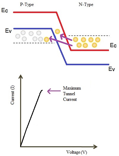
When the amount of voltage applied is increased, the number of free electrons generated at n side and holes at p side is also increased. Due to voltage increase, overlapping between the bands are also increased.
Maximum tunnel current flows when the energy level of n-side conduction band and the energy level of a p-side valence band becomes equal.
Further Increased Voltage Applied to the Tunnel Diode
A further increase in the applied voltage will cause a slight misalignment of the conduction band and valence band. Still there will be an overlap between conduction band and valence band. The electrons move from conduction band to valence band of p region. Therefore, this causes small current to flow. Hence, tunnel current starts decreasing.
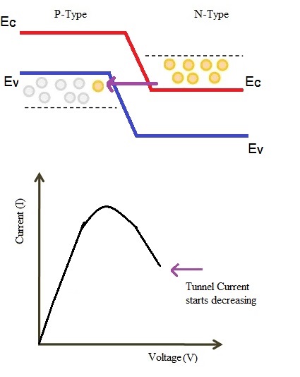
Largely Increased Voltage Applied to the Tunnel Diode
The tunneling current will be zero when applied voltage is increased more to the maximum. At this voltage levels, the valence band and the conduction band does not overlap. This makes tunnel diode to operate same as a PN junction diode.
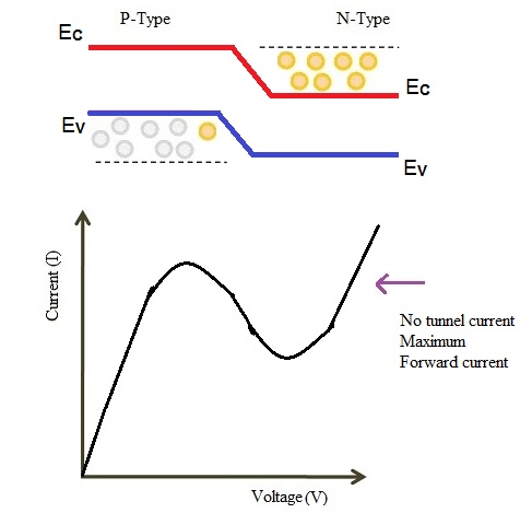
When applied voltage is more than the built-in potential of the depletion layer the forward current starts flowing through the tunnel diode. In this condition, current portion in the curve decreases when the voltage increases and this is the negative resistance of tunnel diode. Such diodes operating in negative resistance region is used as amplifier or oscillator.
V-I Characteristics of Tunnel Diode
Due to forward biasing, because of heavy doping conduction happens in the diode. The maximum current that a diode reaches is Ip and voltage applied is Vp. The current value decreases, when more amount of voltage is applied. Current keeps decreasing until it reaches a minimal value.
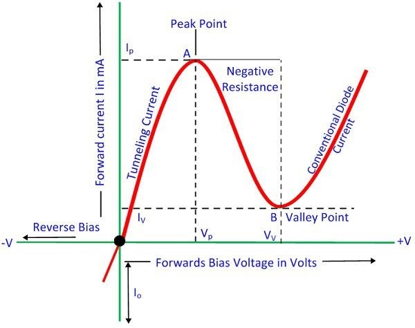
The small minimal value of current is Iv. From the above graph, it is seen that from point A to B current reduces when voltage increases. That is the negative resistance region of diode. In this region, tunnel diode produces power instead of absorbing it.
Applications of Tunnel Diode
- Tunnel diode can be used as a switch, amplifier, and oscillator.
- Since it shows a fast response, it is used as high frequency component.
- Tunnel diode acts as logic memory storage device.
- They are used in oscillator circuits, and in FM receivers. Since it is a low current device, it is not used more.
The post Tunnel Diode – Working, Characteristics, Applications appeared first on Electronics Hub.
from Electronics Hub https://ift.tt/2zhlj80
 Read Part 3 Operational basics, salient features and military specific applications of ring laser gyroscopes and fibre-optic gyroscopes are discussed in this part of the article. Gyroscopic sensors constitute an essential component of inertial navigation sensors (INSes), which are extensively used on a range of aerospace vehicles. These include commercial airliners, military aircraft and spacecraft. Another […]



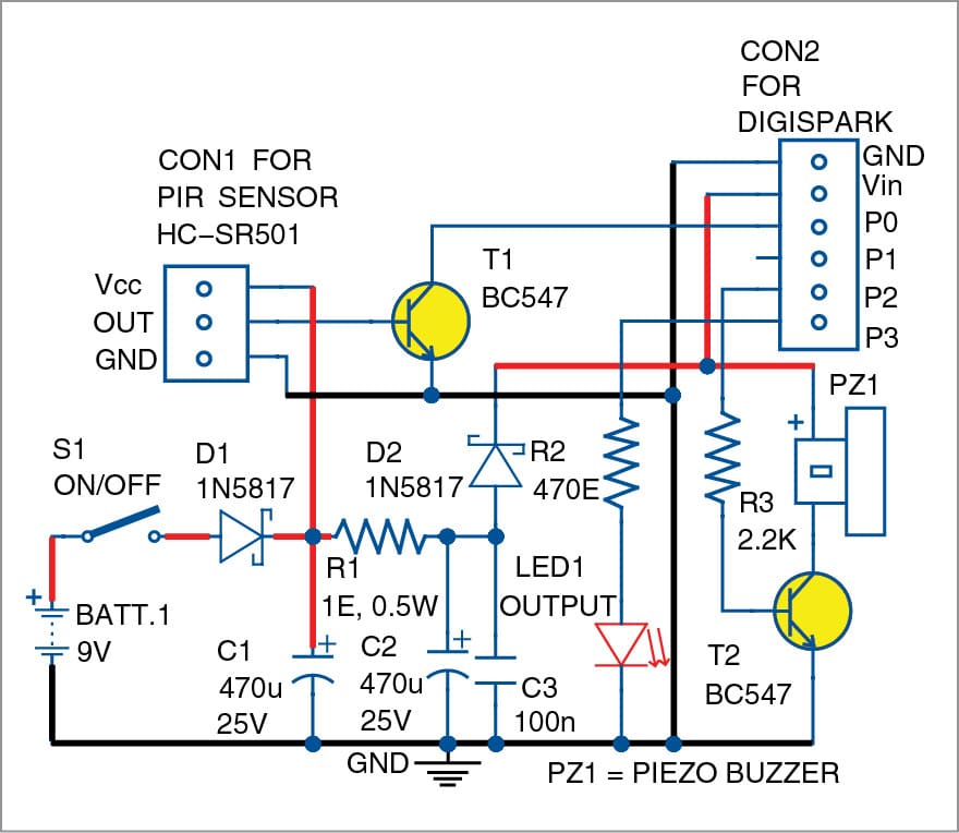 This circuit produces an alarm whenever someone comes near the spotting range of its passive infrared (PIR) motion sensor. It can be used as a security system to guard your home and other property, if utilised properly. The author’s prototype is shown in Fig. 1. Circuit and Working Circuit diagram of the motion detector security […]
 Wi-Fi – a widely used technology for internet connectivity over wireless access. Wi-Fi uses unlicensed spectrum for radio waves, mostly in band of 2.5 GHZ or 5GHz. Wi-Fi has been coping with other wireless access technologies through its rapid advancements. New standards developed by IEEE, has appeared to keep it a relevant technology with time. […]


 In this video, the presenter will be demonstrating how to install an SSD (solid state drive) in a stationary PC. He Is using the SSD as a system drive and leaving the HDD (hard disk drive) as a storage drive. This upgrade will significantly speed up your computer. The operating system will start much faster […]
 A ferrite transformer has a magnetic core in which coil (inductor) windings are made on a ferrite core component. It offers low eddy current losses. It is normally used for high-frequency applications. Common ferrite core types are toroidal, closed-core, shell and cylindrical. Depending on circuit designs, core types and applications of transformers, there are different […]
 Fieldbus is much more sensitive to layout and wiring problems than traditional systems. This webinar is designed to help engineers overcome these challenges to achieve the required performance and reliability to address customer concerns. New Delhi, India –(October 24, 2018)- Mouser Electronics, Inc. in collaboration with Analog Devices, is proud to present technical webinar on […]
 Rome was not built in a day, so wasn’t Amazon Alexa. Key insights from Amazon blog that explain why Alexa keeps getting smarter Amazon Alexa has been the talk of the town since its arrival in the world. Based on voice-commands, it has enabled users to complete a plethora of tasks in much easier and […]
 Read Part 1 Post-silicon validation is an essential step to verify the proper functioning and operation of an SoC, post manufacture. Part 2 discusses elaborately the various methods and parameters involving post-silicon validation. Post-silicon validation involves a number of activities including validation of both functional and timing behaviour as well as non-functional requirements. Each validation […]
 In this video, the presenter will show you how he repaired his lab bench power supply which got damaged through a battery which was connected the wrong way around. Along the way, he will also show you different reverse voltage protection techniques and show you their advantages and disadvantages. Courtesy: GreatScott!
 This article presents a simple circuit to convert transistor-transistor logic (TTL) or pulse width modulation (PWM) signal to analogue signal using LM358 operational amplifier. The circuit can be used as an extension shield for Arduino or microcontroller (MCU) or TTL/CMOS signal generator. PWM-based digital-to-analogue converters (DACs) are often used to produce analogue signals from digital […]
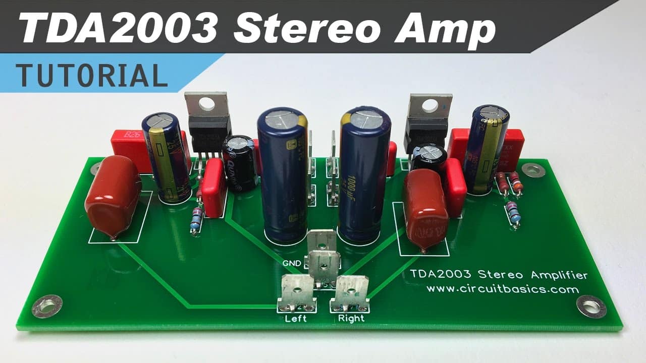 The TDA2003 is a great sounding low wattage chip amp that’s perfect for casual listening with bookshelf and computer speakers. In this video, the presenter is going to show you how to design and build a stereo TDA2003 amplifier. First, he will show you the schematic and talk about what each component does. Then will […]
 All electronic devices and circuitry generate excess heat and, thus, require thermal management to improve reliability and prevent premature failure. Efficiency of an electronic device is inversely proportional to its temperature. A rise in temperature leads to a subsequent drop in performance. High-performance electronic components generate heat loads that create excessive junction temperatures, compromise component […]
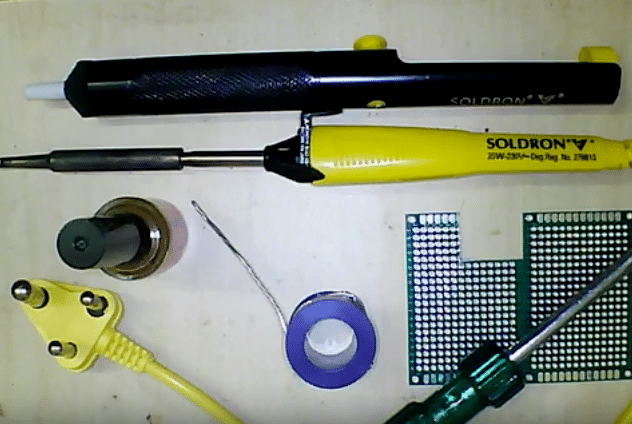 A look around you and you would find yourself within the creative waves emitted by Robotic DIYers (Do-it-yourselfers) who had long followed their inner passion, love and dedication for Robotics. Be it school, college or a corporate scenario you will find such passionate people enjoying their hobby-turned-profession to the fullest. I know you have a […]
 Just like sense organs play an important role in the human body, electronic sensors play a vital role in robotics and artificial intelligence. New and advanced technologies have recreated most human sense organs, or sensors, in robots including eyes, ears, skin and nose. Just like sense organs play an important role in the human body, […]
 Indian banks and enterprises are on a mission to strengthen their security systems against the ever-evolving cyber threats. Sourabh Issar, chief executive officer, CloudSek Information Security Pvt Ltd, tells Paromik Chakraborty of Electronics For You how digital risk management solutions ensure a safe online environment for businesses. Q. How vulnerable are banks and enterprises to […]